ECEN 204 Electronic Design
Test 4
Due 1659 hrs on 22 October 2020.
Name: ………………………………………………………………………
Student Number:……………………………………………………….
Instructions
Attempt al questions
Total = 80 marks
The test will be available on ECS Wiki after 1200 hrs (NZ time) on Wednesday 21 October.
You will have at least 24 hours available to complete and hand in.
Please upload you answer scripts on
ECS Wiki submission system. The submission system
closes at 1659hrs (NZ time) on the 22nd October.
Type or neatly write your answers in the spaces provided. You can also electronically draw
your sketches on the document or else draw in another package and then import into this
document. Show the details of your workings where appropriate – do not just show final
answer.
The test should be completed
individually, that is you may not consult with anyone to
obtain answers but is “open book” – you may consult your class notes/videos or even the
internet.
Save your document with a filename “your surname”_“your initials”_ ECEN204_Test4 and
ensure that you submit this in the ECS Wiki submission system no later than 459 pm (NZ
time) on Thursday 22 October 2020. Please submit as good quality pdf or Word document.
1


All these questions deal with n-type enhancement MOSFETs. Remember, such a MOSFET
will be in saturation mode if: VGS > Vt and VGD < Vt. If the MOSFET is in the saturation
region then: µ
C W
µ
C W
n
ox
2
I
=
(
V
−
V ) and
n
ox
i =
V
(
−
V )
v
D
2
GS
t
L
d
GS
t
gs
2
L
The transconductance is defined by:
i
µ
C W
d
n
ox
g
=
=
(
V
−
V )
m
v
2
GS
t
L
gs
Question 1
[20]
Design the circuit shown in Fig. 1 (i.e. find values for the resistors
RD and
RS) so that the
transistor operates with
ID = 0.4 mA and
VD = +1 V. Assume that
Vt = 2 V, µ
nCox = 20 µA/V2,
L = 10 µm and
W = 400 µm.
VDD = 5 V
ID
RD
I
RS
D
VSS = -5 V
Fig. 1
2
3


 Question 2
[20]
Design the circuit in Fig. 2 to obtain a current ID of 0.4 mA. Find the value required for
R and
find the dc voltage
VD. Assume the values for
Vt, µ
nCox, L and
W as in Q1.
VDD = 5 V
ID
R
VD
Fig. 2
4


 Question 3
[20]
For the circuit shown in Fig. 3 determine if the MOSFET is in saturation mode and find the
drain current. The transistor has
Vt = 2 V and µ
nCoxW/
L = 2 mA/V2.
VDD = 10 V
ID
5.6 kΩ
6.2 MΩ
3.9 MΩ
ID
820 Ω
Fig. 3
5


 Question 4
[20]
For the circuit shown in Fig. 4:
(a) find the dc quantities
ID and
VD;
(b) calculate the value of
gm at this bias point;
(c) calculate the value of the voltage gain.
Assume
Vt = 2 V, µ
nCoxW/
L = 1 mA/V2 and
VGS = 4 V.
VDD = 10 V
ID
3.6 kΩ
+
vgs
V
GS
Fig. 4
*************************************************************************
6
ECEN 204
Assignment 5
Total marks: 40
Below are the problems for this assignment. Do your calculation as needed and then put
your final answers as well any discussion or plots in the spaces required. Submit this
document with a filename:
ECEN204_Assmt5_2021_”your surname”-“your initial” on the Wiki submission system no
later than Monday 4 October by 11.59 pm.
Name: …………………………………………………………………………………………….
Student Number:……………………………………………………………………………….
 Q1.
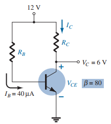
Q1. Given the following figure, determine:
a) IC
b) RC
c) RB
d) VCE.
Answer
(10)
 Q2.
Q2. For the following voltage divider biased amplifier circuit, find:
a) IBQ
b) ICQ
c) VCEQ
d) VC
e) VE
f) VB.
Answer
(15)
Q3. Design a voltage-divider bias network using a supply of 24 V, a transistor with a beta of
110, and an operating point of
ICQ = 4 mA and
VCEQ = 8 V. Choose
VE = 1/8
VCC. Use
standard values.
Answer:
(15)
EEEN 204
Assignment 5
Total marks: 55
Below are the problems for this assignment. Do your calculation as needed and then put
your final answers as well any discussion or plots in the spaces required. Submit this
document with a filename:
EEEN204_Assmt5_2022_”your surname”-“your initial” on the Wiki submission system no
later than Friday 14 October by 11.59 pm.
Name: ……………………………………………………………………………………………..
Student Number:……………………………………………………………………………….
 Q1.
Q1. Given the following figure, determine:
a) IC
b) RC
c) RB
d) VCE.
Answer
(10)
 Q2.
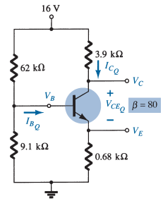
Q2. For the following voltage divider biased amplifier circuit, find:
a) IBQ
b) ICQ
c) VCEQ
d) VC
e) VE
f) VB.
Answer
(15)
Q3. Design a voltage-divider bias network using a supply of 24 V, a transistor with a beta of
110, and an operating point of
ICQ = 4 mA and
VCEQ = 8 V. Choose
VE = 1/8
VCC. Use
standard values and select the components available in the market. Do the second iteration
with the market components and compare the results.
Answer:
(15 + 15
marks for component selection and second iteration of design)
1
Name: ______________________
EEEN 204 Electronic Devices
Test 2: 3 November 2023
There are
50 marks worth of questions in this test. You are to answer all questions and
you have
60 minutes in which to do so. This test is not open book but you are allowed
two sides A4 of hand written notes. If you need additional space then feel free to write on
the back of the pages.
Good luck, have fun.
Unless otherwise stated, you should assume VDD = 5.0 V and that
For nMOS devices
Vt = 1.0 V
Vtd = -3.0 V
For pMOS devices
Vtp = -1.0 V
Vtpd = 3.0 V
𝛽
2
For FETS in saturation, I
ds =
(V
2
gs − Vt)
V2
In non-saturation I
V − V V − ds
DS =
(
gs
t )
ds
2
(1)
Draw the schematic diagram of a pMOS inverter that uses one pMOS enhancement
mode and one pMOS depletion mode transistor.
[3 marks]
(2)
Derive an expression for the steady state
output current of the inverter gate designed
in (1) above, if its output was connected to an identical inverter.
[2 marks]
2
(3)
What
two conditions are required for a
pMOS depletion mode transistor to be
operating in its
saturated mode?
[3 marks] (4)
Name
two elements that could be added as extrinsic impurities to silicon in order to
make it
p-type?
[2 marks] (5)
Draw the block diagram for a CMOS transistor clearly illustrating all the layers.
[2 marks]
3
(6) Calculate the voltage swing of a standard nMOS inverter (one enhancement mode
and one depletion mode transistor) where the pull-up (depletion transistor) has a
L:W ratio of
8:1, and the pull-down (enhancement mode transistor) has a L:W ratio
of
1:1. This is an 8:1 inverter. You may assume that Vin(low) is < Vt, and Vin(high) is
VDD.
[5 marks]
4
(7) What
2 conditions are required for an npn bipolar transistor to be operating in its
saturation mode? Express your answer in terms of VBE, VCB. It is not acceptable
to just state “forward” or “reverse” bias.
[2 marks]
(8) Would a bipolar or a MOSFET transistor be more radiation
immune?
Briefly
explain your answer.
[3 marks]
(9) Determine α and β for a BJT given an emitter current of 5.602 mA and a base
current of 50 µA.
[3 marks]

5
(10)
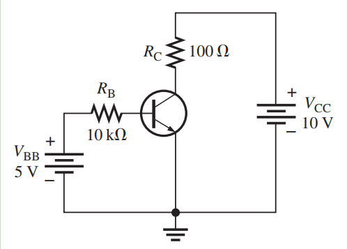
Determine IB, IC, IE, VCE and VCB for
the circuit on the right if βDC = 50.
[7 marks]

6
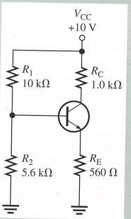
(11) Determine VCE and IC in the stiff voltage-divider based circuit
on the right if βDC = 50.
[8 marks]


7
(12) For the circuit on the right, determine if the
VDD = 10 V
nMOSFET is in saturation mode and find the
drain current ID. The transistor has a threshold
ID
3.6 k
voltage V
6.0 M
t = 2 V and = 2 mA/V2.
[10 marks]
3.0 M
820
ID
Document Outline


